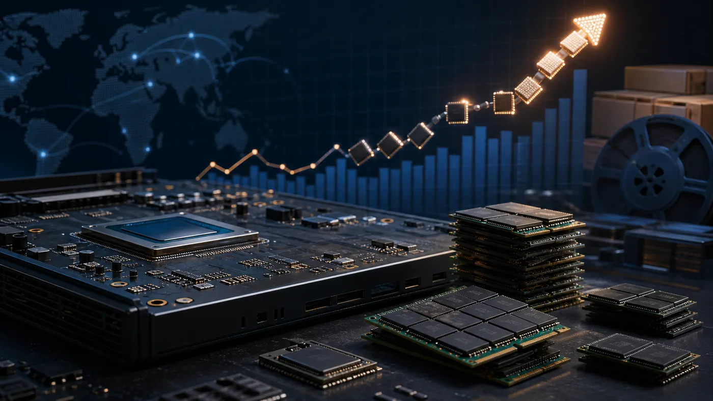
BOE's progress on glass substrate packaging is another sign that the chip industry is looking beyond traditional silicon scaling for performance gains. Advanced packaging has become a core battleground because modern processors increasingly depend on how chiplets, memory, interconnects, and substrates are arranged. A faster transistor is useful, but the system can still be limited by signal loss, power delivery, package warpage, or the difficulty of routing dense connections across large surfaces.
Glass substrates are attractive because they can offer dimensional stability, smoother surfaces, and potential advantages for high-density routing. The technology is difficult, however. Drilling through-glass vias, filling deep holes with copper, building layers, and maintaining yield at panel scale are not simple manufacturing steps. BOE reaching a fully automated equipment flow on a pilot line does not mean mass production is solved, but it does show that the company has moved from concept exploration toward process integration.
This matters for AI chips because advanced accelerators are becoming package-level systems. High-bandwidth memory, interposers, chiplets, optical links, and power delivery all need better substrate options. We have covered the same packaging pressure in custom AI accelerator development, where the real product is often the whole compute module rather than one die.
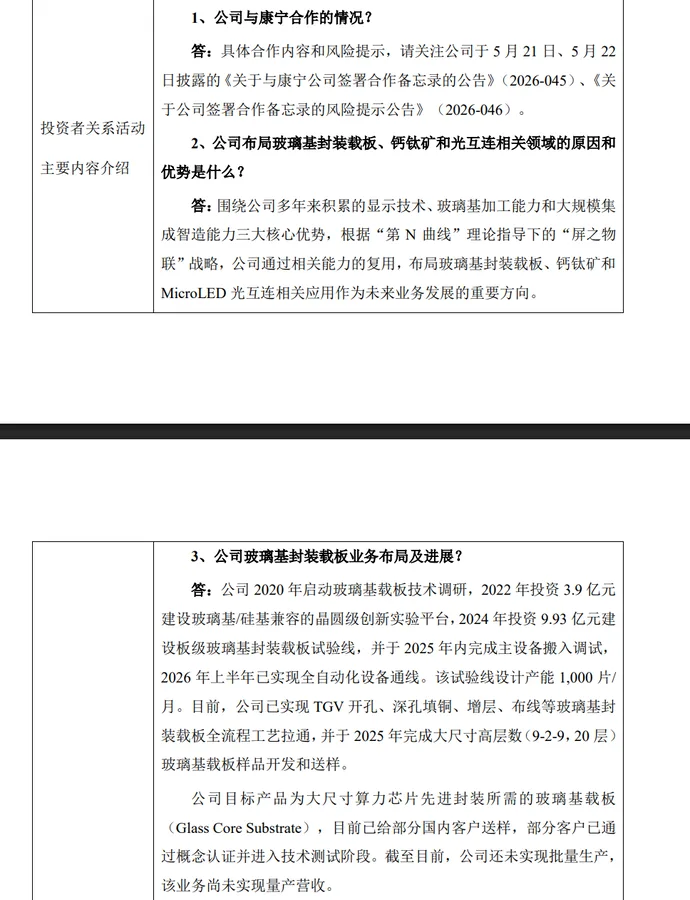
The details reported by IT Home show BOE began researching glass substrates in 2020, invested 390 million yuan in a glass-and-silicon compatible wafer-level innovation platform in 2022, and later invested 993 million yuan in a panel-level glass substrate pilot line. The line has a designed monthly capacity of 1,000 panels and has reportedly completed full-process work including TGV drilling, copper filling, layer build-up, and wiring.
The caution is yield. BOE has previously said the pilot line has not yet reached mass-production yield, and that matters more than demonstration samples. Packaging technology becomes commercially important only when it can be produced reliably, at cost, and with predictable electrical behavior. A 20-layer sample is impressive, but customers will ask about defect density, thermal behavior, long-term reliability, and compatibility with existing assembly flows.
Still, BOE's work is strategically important. Display companies already understand glass, precision manufacturing, large panels, and process control. That background may give BOE a different route into semiconductor packaging than pure chipmakers or OSAT firms. If glass substrates become a meaningful part of AI and high-performance computing packages, companies that can scale panel-level processes may gain a new role in the chip supply chain. The story is not that glass will replace silicon everywhere. It is that packaging is becoming one of the places where the next performance leap may be found.
The commercial path will likely start with targeted applications rather than a sudden industry-wide shift. High-performance computing, AI accelerators, optical interconnect experiments, and specialized modules are better early candidates than cost-sensitive commodity chips. That gives BOE room to prove reliability with partners before chasing large volume. If the company can move yield upward while keeping panel-scale advantages, glass substrates could become one of the more important quiet technologies behind future compute systems. That matters because package substrates increasingly decide how close memory can sit to compute dies, how much power can be delivered, and how far designers can push chiplet layouts before physics turns into cost.